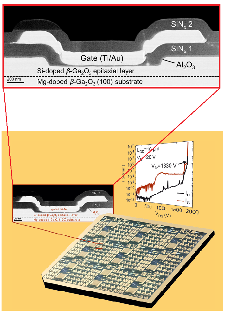
Highlights

TEM imaging of gate topology of a fully processed transistor in

"Lateral 1.8 kV β-Ga2O3 MOSFET With 155 MW/cm2 Power Figure of Merit"

Lateral β-Ga2O3 MOSFET for power switching applications with a 1.8 kV breakdown voltage and a record power figure of merit of 155 MW/cm2 are demonstrated. Sub-μm gate length combined with gate recess was used to achieve low ON-state resistances with reasonable threshold voltages above −24 V. The combination of compensation-doped high-quality crystals, implantationbased inter-device isolation, and SiNx-passivation yielded in consistently high average breakdown field strengths of 1.8–2.2 MV/cm for gate–drain spacings between 2 and 10 μm. These values outperform the results of more established wide-bandgap device technologies, such as SiC or GaN, and the major Ga2O3 material promise — a higher breakdown strength — is well demonstrated.


in IEEE Electronic Device Letters, 40, Issue 9, (2019)

Application of electron tomography for comprehensive determination of III-V interface properties

We present a new analytical method for comprehensive characterization of buried III-V semiconductor interfaces based on electron tomography. Electron tomography uses a large number of two-dimensional images of the sample from different directions - a so-called tilt series - to generate a three-dimensional reconstruction of the layer system. The images are based on the use of a ring-shaped dark-field detector in the scanning transmission electron microscope, which provides a chemically sensitive signal. The image contrast of the individual projections thus obtained satisfies the necessary reconstruction condition. As a case study, the technologically relevant (Al,Ga)As/GaAs multilayer system prepared by molecular beam epitaxy has been used. This consists of a large number of coherent interfaces between layers with different chemical composition and is therefore ideally suited for this type of tomographic investigation. Isoconcentration plots, which are based on the tomogram data and describe the locations of the average concentrations of the contiguous (Al,Ga)As layers, are exploited to obtain topographic height maps of 120 nm x 120 nm area that reveal the interface morphology. The height maps allow the determination of the quadratic roughness of the interfaces, and by applying the height-height correlation function we are able to determine important interface properties such as the lateral correlation length of different interfaces of the (Al,Ga)As/GaAs system. In addition, using height difference maps based on isosurfaces, the 30% and 70% of the total concentration difference at the interfaces, topographic maps of the interface width were generated, from which in turn an average width of the chemical interfacial transition can be calculated. Interfacial tomography quantifies differences in the properties of direct and inverted interface and enables the observation of interfacial anisotropies. The main strength of the methodoligy is the ability to determine all chemical-structural parameters of buried interfaces with the complete three-dimensional data set with one measurement.


in Ultramicroscopy, 224, 113261, (2021)

Funding

The "Application Laboratory Electron Tomography" is funded by the European Regional Development Fund (ERDF) of the European Union and by the State of Berlin (Project No. 2016011843).


Contact

Dr. Achim Trampert Foto
  • Dr. Achim Trampert
  • trampert@pdi-berlin.de
  • +49 (0)30 20377-280
  • Room 615
  • Hausvogteiplatz 5 - 7
    10117 Berlin
    Germany
  • Head of project